Minimize Crosstalk in RF PCBs
As electronic components become more tightly integrated, the interference between signal traces has become a major concern for PCB designers. Unmanaged, crosstalk coupling between signals can override the immunity thresholds of a circuit, causing functional failures. Fortunately, with careful planning, this nuisance can be minimized. This guide explains how to eliminate crosstalk in RF PCBs, and offers best practices to ensure that your hardware performs smoothly.
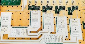
RF PCBs present unique challenges to preventing crosstalk, as higher frequency signal frequencies and faster rise times increase the likelihood of coupling between adjacent traces. Moreover, RF circuits typically feature multiple layers, which can introduce additional complexities and vulnerabilities to the signal integrity of an assembly. In order to avoid this unwanted effect, it’s essential for RF engineers to understand the physics of crosstalk and implement appropriate design rules to minimize coupling between signal layers.
Inter-layer crosstalk is induced by inductive and capacitive coupling between signals that are routed closely together. This interference can cause both the victim and aggressor traces to experience error states. As the error levels reach unacceptable thresholds, they can cause erroneous logic outputs to the circuit’s logic devices. This can lead to system failure, particularly in a clock and periodic signal-driven applications.
How to Minimize Crosstalk in RF PCBs
Crosstalk minimization revolves around ensuring that the far end (FEXT) and near end (NEXT) of the victim signal are not affected by the coupled noise produced by the aggressor trace. To achieve this, a minimum distance, called the 5h design rule, must be provided between two signals. This value translates to a spacing distance between signals that is about an order of magnitude greater than the signal’s effective transmission length.
To reduce the chances of inter-layer crosstalk, a common practice is to use a PCB design tool to determine clearances between the signals during the initial layout. Another solution is to stagger the signal layers in a PCB. Finally, it’s also important to design a PCB with solid ground planes between the signal layers. These shields prevent signals from coupling through cutouts, antipads, and other gaps in the layer stack.
Lastly, minimizing inductive and capacitive coupling is crucial for eliminating crosstalk in rf pcb. This can be achieved by making sure that traces are properly spaced and routed. For example, traces should not be placed parallel to each other as they can interfere with each other’s magnetic fields. To further minimize interference, a PCB designer should also make sure that signal-layer traces are separated by amplitude.
To reduce interference, PCB designers must carefully guard their traces with copper planes and shielding materials. In addition, they should ensure that traces are spaced apart and avoid congested layouts. They should also minimize right-angle bends, as these can cause impedance mismatches between traces and cause them to couple. Additionally, RF engineers should consider using wider traces to lower inductive coupling. With the help of these simple strategies, RF engineers can mitigate crosstalk in RF PCBs and ensure that their devices operate as intended.